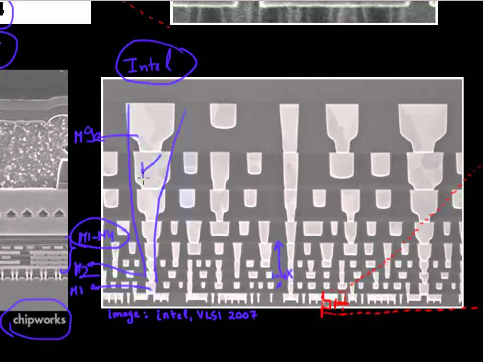
Hello folks in these next set of videosI’ll be describing to you about the process technology of thedifferent steps which are involved in making the chips that you see on your ipad or youriphone or your laptop computer And we will be going into pretty gory detailsof how these chips are made. What are the different steps involved. But before I get into the nitty-gritty ofthat, I want to give you a feel of how these actual chips look whenyou open them up. So if you open up say a micro processor or your memory chip what does it actuallylook like? If you take a picture from the top, or ifyou take a cross section view.So, I want to just briefly describe to you in this video thatabout three of these chips. The first being the microprocessor. Or this A5X microprocessor that you see inyour iPad. And then the second chip I want todescribe to you is this DRAM chip. And the third chip I want to describe isthis NAND flash memory. And these are the typical three componentsthat you see in any mobile devices. You always find a microprocessor. You always find a DRAM chip.This DRAM chip sometimes is stand alone. Sometimes it’s actually stacked on top ofyour microprocessor. To save a space on your board and youalways find almost always find a NAND flash memory to store yourapps and store your data as well. So let’s start with this micro processor,so if you open up this micro processor and look at its die thisis what it looks like.So these are shown here are threegenerations of these microprocessor chips starting fromA4 to A5 to A5X. And then interesting observation about these diesis that more than 50% of the area here, or more than half of the area on this die is covered by these Is occupied by, by these SRAMcells. So if you take ten pictures of on thisdie from the top there’s a large chance that five of themwould look something like this. So shown here is a six transistor SRAM cell.So shown here is one of these unit cells which is six transistor SRAM cells.And shown here is, is the, is the circuit diagram for the cell.So this SRAM cells is is essentially consist of six transistors two of them it consists two ofthese inverters. One of them drawn in green and the other one drawn in blue and they are crossconnected. And then you have these two pass-gatetransistors which connect which are used to essentially read the state of the cell.So if, if you look at this picture over here.You know one, one does this looks nothing like the second diagramso where are these transistors located.So let me help you out a little bit, so let me help you out in locating thesetransistors. So these these parallel lines over herethese are essentially the gate lines. And these perpendicular lines over here,these are the active lines. So shown here are the, these two set oflines, one of them are the gate and the other one areactive area. And so now let’s, let’s try and look atthese transistors. So we see that this inverter has aninverter here, so the gate of these two transistors mustbe connected. And they must be connected to the sourcedrain of these other two transistors. So two of these transistors which areshown in green over here, they can be located overhere. So there’s a gate line running over here.So this is one of these transistors and this is the other of these greentransistors. And then the gate of this is connected to the source and drainof these second inverter. And also the source drain of these two are connected, so these two would beconnected. this would be on another layer which isnot shown over here. And let’s look at this other inverters, sothis other inverter in blue could be drawn over here.So there would be this gate and this gate line is not in common so thiswould be the other transistor. And then they are connected to the sourceand drain all this first first inverter. And then the source and drain of thesecond inverter would be connected too. And the gate of this first inverter wouldthen connect to the source drain of the second inverter. So, as shown here are two inverters. And then they are connected using these pass-gate transistors, which are locatedover here. So, this is the pass, first pass-gate transistor, and this is the secondpass-gate transistor. So, now, now we have been able to locate these are, these are, these are twopass-gate transistors.And then there are these, two invertersso, this is how the, the circuit diagram translates onto thistop view. And, this is the most compact way you canyou can pack these six transistors into youronto your die. Now that we have enjoyed the aerial view,let’s look at side view so lets if we take a cross section ofthis die. So if we take a cross section of this dieand look at it side ways this is how it looks like, so this is a Image courtesy from chipworks. And, it shows how, how this looks likefrom the side. So you can again see these individual transistors which would be somewhere overhere.And then you have these vias which areconnecting this transistor to these interconnectlines. So you see multiple of these interconnectlines. metal 1, metal 2, metal 7. And these are essentially routing all thesignals between these SRAM and then your logic circuitry.And so on and so forth. And this is, this is showing across-section view of A5 microprocessor from your iPad.If you take a cross-section of your chip that is on yourlaptop. So this is showing a cross-section view ofof Ivy Bridge processor, similar to Ivy Bridge processor from Intel.So this is how it would look like, again you have your transistor locatedsomewhere over here.And then you have again these multiplemultiple levels of interconnects. So this would metal one, metal two, allthe way up to I think they have nine levels ofthese interconnects. And these interconnects are slightlydifferent between your, between your A5microprocessor and the chip from Intel.So the chip A5 microprocessor you see that there are these two sets of pitches between your interconnects.All your metal 1 to metal 4 have 1 pitch. And then the layers above them have.uh,another pitch. And in the Intel microprocessor, you seethat all of the levels of metals have different pitch.So if the pitch here is x, the pitch hereis maybe 1.4x. And then the pitch of each of theseinterconnects is continuously increasing as can be shownon here. because they want to optimize, reallyoptimize the performance uh.u or minimize the delay that you get fromyour interconnect. So this is really optimized forperformance to the very core. Where our, over here you are just livingwith maybe two or three levels of pitches for your metalinterconnect. So again you you if you really zoom inover here, you can locate these transistors are shown here isa 32nm transistor from Intel. And over here you can see the source andthe drain. And this is the gate and there’s a Hi-Klayer, Hi-K Hi-K layer over here.And then these are the contact, these are the contact plugs, which are connectingyour source and drain and connecting them to the inter, theinterconnects above.We took a look at the microprocessor chip.So now let’s examine the DRAM DRAM chip.So if you open up a DRAM die, this is how it looks like.So most of the area on your DRAM chip is occupied by these banks ofmemory. So each of them has many of these DRAMcells. Each DRAM cell is essentially a one transistor, one capacitor cell. And you have eight of these DRAM banksshown over here. In the middle also you have thiscontroller, circuitry. So what this controller circuitry does is it takes the command from yourmicroprocessor. And it decodes into this column addressand this row address. To go and read that, read or write thatparticular set. And so majority of the area over here isoccupied by this banks of cells. And so if you, if you, if you took a crosssection. There’s a very large percentage that youwill end up on a something which looks likethis. And, the first thing that, you know, you,if you look at this cross section is, is gee, you know, whatthe heck is this, you know? So it, it looks something like eitherantenna hanging in the sky or it looks like this looks like ahorn of a deer, right? So they.It looks like either antenna or horn of adeer so What is this you know we were supposed to havethis nice one transistor one capacitor. So where are where is the transistor firstof all. So if you look very carefully thetransistor is located somewhere over here. So, you’ll have your transistor locatedsome were over here. So, this is your access transistor. And this antenna or these set of horns hanging in the sky these areactually the capacitor. So, the way a DRAM cell works let me give you a very quick intro.So the way a DRAM cell works is that you store a charge on this capacitor.And then you have this access transistor whose purpose is to essentiallyhelp access the charge on this capacitor. So the capacitor is charged and you turnthis transistor on.That charge will get transferred on this,bit line. And then you sense that voltage increasein the bit line due to this charge. And that’s how you read the state of thisset. So, a few requirements on on thiscapacitor that you wanted to have as high of a capacitance, aspossible. So it can store a large quantity ofcharge. On this transistor, one of the mainrequirement is, it should have low off current so that the dischargewhich is stored in your . In your capacitor does not leak awaythrough this transistor. So this antenna is this capacitor, and it, it’s a MIM capacitor, so you have ametal, and you have an insulator, and you haveanother metal.So if, if you take a more closer look at this, it on this capacitor, it lookslike this. So you have two of these metal layers. So you have one of these metal layerswhich is Ti-nitride. So you have one layer of trinitride here,you have another of this metal layer, so this is two metal layers.Metal and then other metal layer, both of thembeing Ti-nitride And in between you have this insulatorlayer. So in between you have this Aluminumoxide, which is an insulator, and that essentiallymakes up this transistor. Make up this capacitor.So again, if you take a top view it would look something like this.So you have the multiple of these antennas or horns hanging up in the sky.So you want to make the capacitor as capacitance of this capacitor as largeas possible.So one way to do that is essentially to increase the height of the antenna. So you can keep it increasing makingtaller and taller But again one of the challenges there is that thesestructure should not collapse. If they collapse they will short eachother so you definitely don’t want that to happen.And the way its design like an antenna again to maximise this capacitance soshown in this cartoon are a. Is this one transistor one capacitordesign. So you have a transistor over here whichis an access transistor and then you havethis capacitor.And this this is called a stacked capacitordesign because your capacity is stacked on top ofyour transistors. And again one way to increase the, thecapacitance is to increase the surface area of thiscapacitor. So one way to increase the surface area isto essentially hollow this capacitor out. And now you get both surface area on theoutside and you get surface area on the inside.So that’s why a design like an antenna.So you get both the surface area on theoutside and then you get the surface area on theinside. And sometimes you’re actually roughen thesurface as well. So you make the surface rough becauseessentially again that increases your surface area which increases thecapacitance of this capacitor..